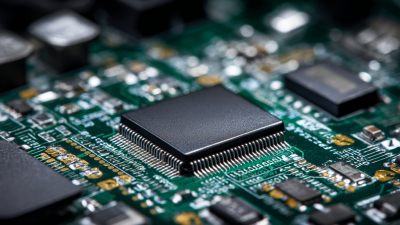
2025 Top 5 Printed Circuit Board Assembly Innovations to Watch
 The landscape of printed circuit board assembly (PCBA) is evolving rapidly, driven by technological advancements and increasing demand for high-performance electronics. According to a report by MarketsandMarkets, the global PCB market is projected to reach $85.3 billion by 2024, with the assembly segment playing a crucial role in this growth. As industries such as automotive, consumer electronics, and medical devices continue to innovate, the need for advanced PCB assembly techniques becomes more critical, positioning the PCBA sector at the forefront of electronic manufacturing evolution.
In 2025, several groundbreaking innovations are anticipated to reshape the printed circuit board assembly landscape. From enhanced automation processes to the integration of artificial intelligence for quality assurance, these advancements promise to boost efficiency and precision in manufacturing. The implementation of advanced materials and the rise of miniaturization trends will also drive the development of more compact and powerful electronic components. As PCBA technology continues to advance, manufacturers must stay ahead of these trends to meet the growing demands of a competitive market and ensure the reliability and performance of their products.
Emerging Trends in PCB Assembly Automation and Efficiency Enhancements
 The landscape of PCB assembly is poised for significant transformation through the integration of automation and enhanced efficiency strategies. Emerging technologies such as generative AI and advanced data analytics are spearheading this change, enabling manufacturers to streamline their processes, reduce costs, and improve product quality. Automation not only increases the speed of assembly lines but also enhances precision, minimizing human error and waste.
As the industry evolves, the adoption of IoT and machine learning will further drive innovations in PCB assembly. These technologies facilitate real-time monitoring and predictive maintenance, ensuring optimal operational performance. Moreover, the focus on sustainable practices and energy efficiency is compelling manufacturers to invest in smarter automation solutions. In this dynamic environment, staying abreast of technological trends will be crucial for businesses aiming to remain competitive in the ever-evolving electronics manufacturing landscape.
Innovative Materials Revolutionizing PCB Durability and Performance
As the electronics industry continues to evolve, 2025 promises groundbreaking innovations in Printed Circuit Board (PCB) assembly, particularly in the realm of materials that enhance durability and performance. Recent reports from the IPC (Association Connecting Electronics Industries) highlight a shift towards advanced polymer composites and ceramic materials, which are set to greatly increase thermal resistance and mechanical strength of PCBs. With the increasing demand for electronics in harsher environments, such as automotive and aerospace applications, these innovative materials are becoming crucial in ensuring longevity and reliability.
Tip: When selecting PCB materials, consider the specific environmental challenges they will face. High-temperature applications may benefit from polyamide or liquid crystal polymers, which offer excellent thermal stability.
Moreover, the integration of nanotechnology into PCB materials is also gaining traction. Utilizing nanomaterials can lead to thinner, lighter PCBs without compromising on strength or electrical performance. According to a study by Research and Markets, the global PCB market is expected to reach $82.3 billion by 2025, partly driven by these advancements in material science.
Tip: Stay informed about the latest material innovations and consider prototypes to test their performance in real-world applications, potentially reducing failures and enhancing product reliability.
2025 Top 5 Printed Circuit Board Assembly Innovations to Watch
| Innovation |
Description |
Key Benefits |
Estimated Impact |
| High Thermal Conductivity Materials |
New composites designed for better heat dissipation. |
Enhanced thermal management, reduced risk of overheating. |
Increased reliability and lifespan of electronic components. |
| Flexible PCBs |
PCBs that bend and flex without breaking. |
Design flexibility, lightweight applications, better integration. |
Widely applicable in consumer electronics and wearable devices. |
| Eco-Friendly Materials |
Biodegradable and recyclable PCB materials. |
Reduced environmental impact, compliance with regulations. |
Positive brand image and market appeal. |
| 3D Printed PCBs |
Additive manufacturing techniques for circuit boards. |
Rapid prototyping, reduced material waste, design customization. |
Faster time-to-market for new products. |
| Automated Inspection Technologies |
AI and machine learning integrated for quality control. |
Enhanced accuracy, reduced human error in inspections. |
Higher production quality and yield rates. |
The Impact of AI and Machine Learning on PCB Design and Production
As the influence of AI and machine learning continues to reshape the landscape of PCB design and production, innovative tools and techniques are emerging. The integration of advanced AI algorithms is enabling more efficient design processes, allowing engineers to optimize board layouts and enhance performance while reducing material waste. This shift is critical, especially given the projected growth in the PCB testing equipment market, which is expected to expand significantly by 2033.
Tips: When exploring PCB design enhancements, consider leveraging tools that incorporate AI-driven simulations. This approach can help streamline your workflow, identify potential design flaws early, and ultimately save time and costs.
Moreover, the off-line PCB laser depaneling systems market is set for steady growth, reflecting the increasing need for precise manufacturing techniques. As these systems gain traction, they contribute to higher production standards and more consistent quality in PCB assemblies.
Tips: Keep an eye on emerging technologies that enhance the efficiency of PCB manufacturing processes. Investing in modern equipment can lead to long-term benefits, including reduced turnaround times and improved accuracy in your projects.
Sustainable Practices in PCB Manufacturing: The Rise of Eco-friendly Solutions
The rise of eco-friendly solutions in PCB manufacturing is gaining momentum, as businesses increasingly recognize the importance of sustainable practices. A recent report from the IPC (Association Connecting Electronics Industries) highlights that up to 70% of manufacturers are shifting towards sustainable materials and processes to reduce their environmental impact. This trend not only caters to the growing demand for sustainable electronics but also aligns with global initiatives aimed at reducing carbon footprints in the electronics industry.
One innovative practice emerging in PCB assembly is the use of bio-based materials. These materials, derived from renewable resources, significantly lower the carbon emissions associated with traditional material production. According to a study by Research and Markets, the global market for green electronics is expected to surpass $1 trillion by 2025, further emphasizing the critical nature of this shift. Additionally, implementing closed-loop processes in PCB design and production can help minimize waste, with companies reporting waste reduction of over 40% through optimized recycling strategies. Manufacturers focusing on these eco-friendly innovations are not just enhancing their brand image but also positioning themselves for compliance with future regulations on environmental sustainability.
Advancements in Connectivity Technologies Driving PCB Functionality in IoT Applications
As we look toward 2025, the landscape of printed circuit board (PCB) assembly is set to undergo significant transformations, especially driven by advancements in connectivity technologies. With the rise of the Internet of Things (IoT), the demand for PCBs that can seamlessly integrate with various connected devices is becoming critical. These innovations focus on enhancing communication protocols, developing smart materials, and implementing miniaturization techniques that allow for more complex functionalities within limited space.
Tips: When considering PCB design for IoT applications, prioritize flexibility in circuit layouts. This adaptability can facilitate quicker iterations and modifications, aligning with the fast-paced evolution of IoT technology. Additionally, staying updated on the latest communication standards can ensure compatibility with emerging devices.
Moreover, the utilization of AI and machine learning in PCB assembly processes is expected to streamline production efficiency and reliability. These technologies can predict potential failures, optimize manufacturing workflows, and enhance quality control, ultimately leading to faster time-to-market for IoT devices.
Tips: Leverage AI-driven tools that analyze production data in real-time. By integrating these solutions, manufacturers can not only enhance efficiency but also improve decision-making, allowing for proactive problem resolution throughout the PCB assembly process.