2025 How to Design an Electronic Circuit Board: Step-by-Step Guide
Designing an electronic circuit board (ECM) is a fundamental skill in the realm of electronics, underpinning everything from simple gadgets to complex machinery. As the backbone of electronic devices, an electronic circuit board facilitates the flow of electrical signals, ensuring that components work harmoniously together. This step-by-step guide aims to demystify the process of circuit board design, providing you with the insights and techniques to create functional and efficient boards.
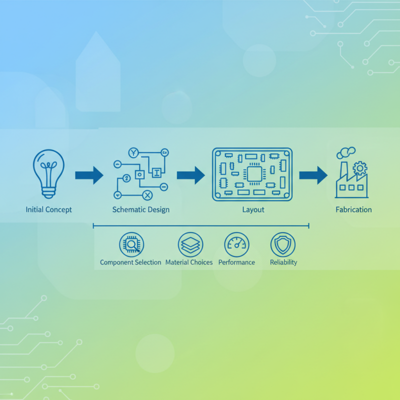
In today's fast-paced technological landscape, understanding how to design an electronic circuit board is essential for engineers, hobbyists, and innovators alike. This guide will walk you through the critical stages of the design process, from initial concept and schematic design to layout and fabrication. You'll learn about key considerations, including component selection and material choices, that influence the performance and reliability of your circuit board. By mastering these concepts and techniques, you will be equipped to bring your electronic ideas to life, ensuring your designs are not only effective but also feasible for production.
Understanding the Basics of Electronic Circuit Board Design
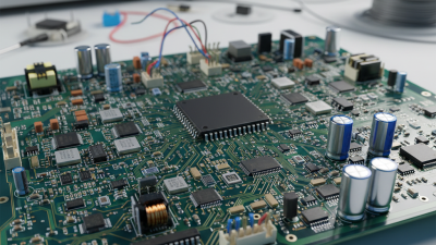
Understanding the basics of electronic circuit board (PCB) design is essential for anyone looking to venture into the world of electronics. At its core, a PCB is a platform that provides physical support and electrical connections for electronic components. It consists of a flat sheet of insulating material, usually fiberglass or composite epoxy, onto which conductive pathways are etched or printed. These paths, typically made of copper, allow electric current to flow between components such as resistors, capacitors, and integrated circuits, enabling the entire circuit to function effectively.
To begin designing an electronic circuit board, one must first understand the schematic diagram, which serves as a blueprint for the PCB layout. This diagram outlines the components and their connections, providing a clear visual representation of how the circuit will operate. Once the schematic is established, the next step is laying out the PCB, taking care to consider factors such as component placement, trace routing, and ground planes. It’s important to optimize the layout for performance, minimizing interference and ensuring reliable power distribution. Understanding these fundamentals will pave the way for successful PCB design, setting a strong foundation for more advanced techniques in the future.
2025 How to Design an Electronic Circuit Board: Step-by-Step Guide
| Step |
Description |
Tools Needed |
Estimated Time |
| 1 |
Define the purpose of the circuit board |
None |
1-2 hours |
| 2 |
Create a schematic diagram |
Schematic capture software |
2-3 hours |
| 3 |
Select components |
Catalogs, online databases |
1-2 days |
| 4 |
Layout the circuit board |
PCB design software |
3-5 days |
| 5 |
Prototype the circuit board |
PCB manufacturing service |
1-2 weeks |
| 6 |
Test and validate the design |
Testing equipment |
1 week |
Selecting the Right Materials for Your Circuit Board
When designing an electronic circuit board, selecting the right materials is crucial to ensure optimal performance and longevity. The choice of substrate is fundamental, as it affects both the mechanical properties and electrical characteristics of the board. Common materials like FR-4, a fiberglass-reinforced epoxy laminate, are popular due to their excellent strength and thermal stability. However, for high-frequency applications, materials such as PTFE (polytetrafluoroethylene) might be more suitable, offering lower dielectric losses.
In addition to the substrate, the choice of copper thickness is another vital consideration. Thicker copper can handle higher currents, making it essential for power circuits. Conversely, thinner copper layers are often used in high-density designs where space is limited. The use of protective coatings, such as solder masks and conformal coatings, is equally important to prevent corrosion and ensure reliable soldering. Ultimately, understanding the intended application and environmental conditions will guide the selection of materials, leading to a more effective and durable circuit board design.
Electronic Circuit Board Material Selection: A Comparative Analysis
This chart illustrates the comparison of different materials used in electronic circuit boards, highlighting their properties such as conductivity, durability, and cost. The data helps in understanding which materials are most suitable for specific applications.
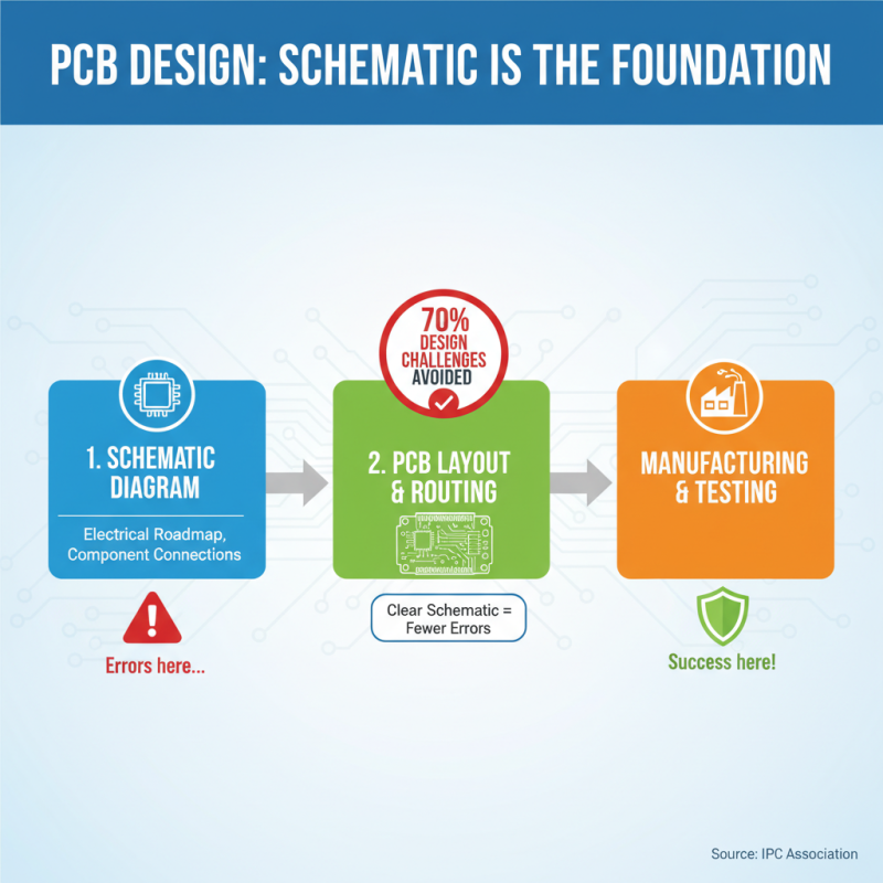
Creating a Schematic Diagram: The First Step in PCB Design
Creating a schematic diagram is an essential initial step in the electronic circuit board (PCB) design process. This diagram acts as a roadmap for engineers, visualizing the electrical connections and functionalities of components. According to a report by the IPC Association Connecting Electronics Industries, approximately 70% of design challenges stem from errors that could have been avoided with a clear schematic. Therefore, investing time in crafting a precise and detailed diagram is critical to the overall success of the PCB design.
The process of creating a schematic involves several key elements. First, selecting appropriate symbols for electronic components is crucial—these symbols must conform to industry standards to ensure consistency and clarity. As per the 2022 Design and Manufacturing Report, standardized symbols help reduce miscommunication among team members, ultimately leading to fewer revisions during later stages of the design process. Moreover, modern design software often provides libraries of standardized symbols, streamlining the schematic creation process. Once the schematic is complete, it allows for simulation and validation of electrical performance, allowing designers to identify potential issues before moving to layout and fabrication stages, thereby enhancing efficiency and reducing costs.
Layout Techniques: Arranging Components for Optimal Performance
Effective layout techniques are crucial for designing an electronic circuit board (PCB) that delivers optimal performance. One of the key considerations in PCB design is the proper arrangement of components to reduce design errors and enhance signal integrity. According to a report by IPC (Institute for Interconnecting and Packaging Electronic Circuits), improper component placement can lead to performance issues that cost the electronics industry billions in annual reworks and failures. Therefore, adhering to best practices in component layout is essential for preventing such losses.
When arranging components on a PCB, it is vital to prioritize the placement of sensitive components and high-speed signals. Placing components that interact frequently in close proximity can minimize the lengths of signal paths, thus reducing latency and electromagnetic interference. Data from the IPC reveals that optimal component placement can improve signal integrity by up to 30%. Additionally, designers should consider using ground planes and proper routing techniques to prevent crosstalk and ensure efficient heat dissipation, as thermal management plays a significant role in the longevity and reliability of electronic devices. By focusing on these layout strategies, designers can significantly enhance the performance and robustness of their electronic circuit boards.
Testing and Troubleshooting Your Finished Circuit Board
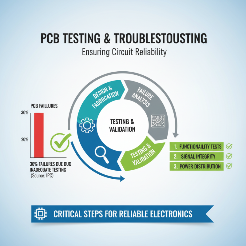
Testing and troubleshooting are critical steps in the life cycle of an electronic circuit board (PCB). After designing and fabricating a PCB, engineers must ensure that every component functions as intended. According to a report by the IPC (Association Connecting Electronics Industries), nearly 30% of all PCB failures stem from inadequate testing processes. This statistic emphasizes the importance of implementing thorough testing routines that include functionality tests, signal integrity analyses, and power distribution assessments, which are vital to ensuring the reliability and effectiveness of the circuit.
A systematic approach to troubleshooting can save both time and resources. Utilizing methods such as boundary scan testing and in-circuit testing allows engineers to identify faulty components quickly. The IEEE Standards Association states that employing such measures can reduce debugging time by nearly 50% compared to traditional methods. Furthermore, adopting software tools for simulation and analysis can help visualize potential issues before physical testing. By adhering to industry standards and best practices, engineers can effectively troubleshoot circuit boards, ensuring optimal performance and minimizing long-term costs associated with failures.