WORLD electronics offers a complete line of electronic circuit board manufacturing and assembly services, as well as advanced manufacturing services. Our commitment to quality and service is second to no supplier.
Learn MoreOur team of engineers assists you in the development of new designs to optimize quality manufacturability (DFM) and testability, resulting in cost minimization and reduced product development time.
Learn MoreOur flexible manufacturing floor layout and highly trained staff allow for Quick Set-up and Tear Down of small volume prototype runs. This combination grants our customers the benefit of turning new designs quickly and accurately.
Learn MoreWORLD electronics is dedicated to quality. This quality is what underpins our commitment to thorough testing. Our engineers can develop a set of tests that ensure reliability and high performance in all products.
Learn MoreSupply chain management has crossed over from being a narrow management function to being a key operational function.
Learn More
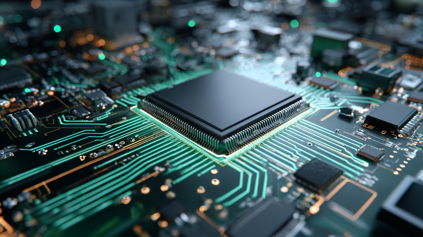
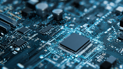
In today's fast-paced technological landscape, the design of an electronic circuit board (PCB) plays a crucial role in the functionality and reliability of various electronic devices. According to a report by Mordor Intelligence, the global PCB market is projected to reach $85.8 billion by 2026, driven by the increasing demand for sophisticated electronic equipment in sectors such as consumer electronics and automotive. As the complexity of modern PCBs escalates, engineers face the challenge of optimizing their designs for both performance and manufacturing efficiency. Effective PCB design not only enhances signal integrity and minimizes electromagnetic interference but also streamlines production processes. This blog will explore best practices and innovative techniques for designing electronic circuit boards that ensure optimal performance, addressing common pitfalls and leveraging advanced technologies to meet the ever-growing demands of the industry.
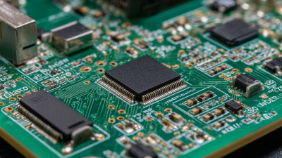
When designing an electronic circuit board (PCB), understanding the fundamental design principles is crucial for achieving optimal performance. A well-designed PCB can significantly impact the efficiency and reliability of electronic devices. According to a report by IPC, the global standards and trade association for the electronics industry, nearly 60% of electronic product failures are attributed to poor PCB design. This emphasizes the importance of adhering to design guidelines that enhance signal integrity, minimize electromagnetic interference (EMI), and ensure thermal management.
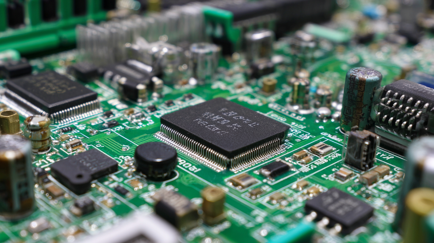
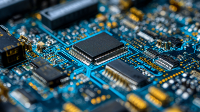
One key principle is the effective layout of components and traces to reduce the length of connections, which helps minimize resistance and inductance. Research from Mentor Graphics reveals that a reduction in trace length can lead to an improvement in signal integrity by up to 30%. Additionally, the use of proper grounding techniques and decoupling capacitors can stabilize voltages and provide necessary power to components. Studies show that implementing these strategies not only enhances performance but can also extend the lifespan of electronic products, ultimately benefiting manufacturers by reducing warranty costs and enhancing consumer satisfaction.
When designing an electronic circuit board (PCB), the choice of components and materials plays a crucial role in achieving optimal performance. Key components such as resistors, capacitors, and integrated circuits must be selected not only for their electrical characteristics but also for their compatibility with the overall design. For instance, using high-quality capacitors can improve signal integrity and reduce noise, while precision resistors can enhance the stability and accuracy of the circuit. Additionally, understanding the specifications and limits of these components helps engineers avoid potential failures and ensures longevity.
Equally important are the materials used in PCB manufacturing. The substrate material, often made of fiberglass or epoxy resin, significantly impacts the board's thermal and electrical performance. FR-4 is a common choice due to its excellent dielectric properties and reliability. Conductive materials, usually copper, must be carefully plated to ensure good conductivity and durability. Furthermore, surface finishes like HASL or ENIG can protect the copper from oxidation while providing a solderable surface for components. Selecting the right combination of components and materials is essential for achieving the desired performance and reliability in electronic circuit board design.
Key Component | Function | Material Used | Performance Impact |
---|---|---|---|
Resistor | Limits current flow | Carbon film | Affects signal quality |
Capacitor | Stores electrical energy | Ceramic | Improves stability |
Inductor | Stores magnetic energy | Air core | Controls frequency response |
Transistor | Amplifies current | Silicon | Critical for gain performance |
PCB Material | Supports circuit components | FR-4 | Affects thermal management |
Solder | Connects components | Lead-free alloy | Influences joint reliability |
When designing an electronic circuit board (PCB), analyzing electrical performance metrics becomes paramount to achieving optimal circuit function. Key metrics such as signal integrity, power distribution, and thermal management play crucial roles in ensuring the reliability and efficiency of the PCB. Signal integrity refers to the quality of the electrical signals transmitted across the board, which can be affected by factors like impedance mismatches and crosstalk. Evaluating these aspects through simulations and measurements can help identify potential issues early in the design process.
Power distribution is another vital metric that impacts the overall performance of the circuit. An effective power distribution network (PDN) ensures that all components receive stable voltage and current, minimizing fluctuations that could lead to malfunctions. Designers must consider factors such as trace width, copper thickness, and the placement of decoupling capacitors to optimize the PDN.
Additionally, thermal management cannot be overlooked, as excessive heat can degrade performance and shorten the lifespan of components. Implementing proper heat sinks, thermal vias, and airflow considerations can significantly enhance the thermal performance of the circuit board, contributing to long-term reliability and functionality.
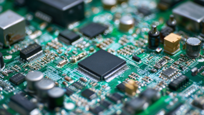
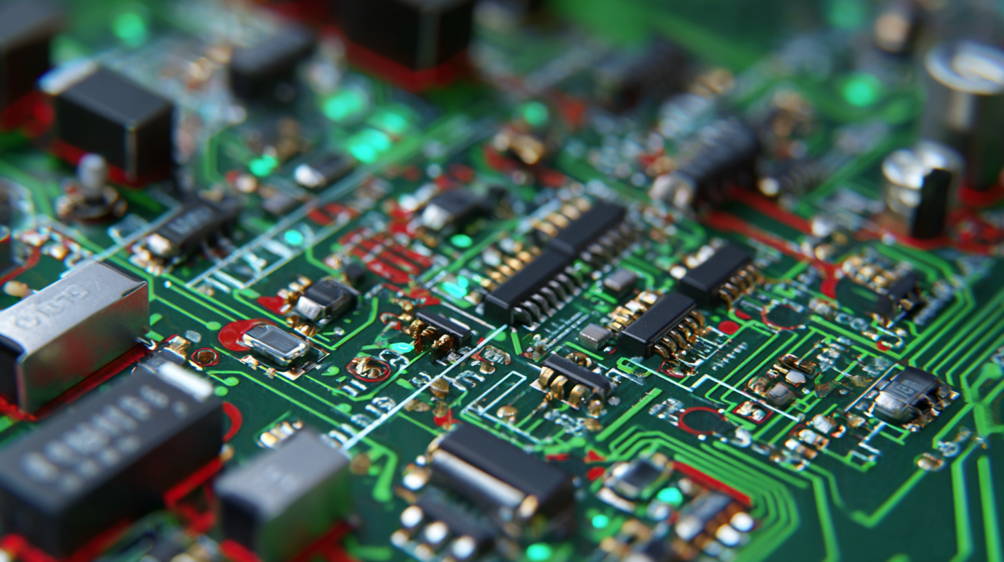
When designing an electronic circuit board (PCB), the layout and routing are crucial for achieving optimal performance. Best practices for these elements can significantly influence the functionality and longevity of a PCB. First and foremost, maintaining an organized and straightforward layout allows for improved signal integrity and reduces electromagnetic interference (EMI). Designers should prioritize the placement of components in a manner that minimizes the distance between related parts, which not only helps in reducing parasitic inductance and capacitance but also simplifies the overall routing process.
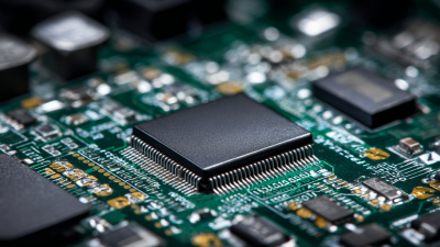
Moreover, effective routing techniques should be employed to facilitate seamless communication between different circuit elements. It's essential to use wider traces for high-current paths to prevent overheating and voltage drops. Additionally, implementing ground planes and using differential pairs when dealing with high-frequency signals can dramatically enhance performance. Designers should also be mindful of the via placements, ensuring they are not overly congested, which can lead to signal distortion. By adhering to these best practices in layout and routing, one can create a robust PCB that meets the desired operational specifications while minimizing potential issues.
When designing electronic circuit boards for optimal performance, testing and troubleshooting are critical steps that cannot be overlooked. One of the most effective testing techniques is the use of oscilloscopes and multimeters. These tools allow engineers to visualize voltage fluctuations and current pathways, helping to identify any anomalies in circuit behavior. Regularly monitoring signal integrity throughout the design process also ensures that unexpected interference or signal degradation can be addressed early on, preventing costly errors in later stages.
In addition to visual testing methods, implementing functional testing is essential. This involves applying power to the circuit and verifying that it operates as intended under various conditions. A systematic approach to troubleshooting can be achieved with the “divide and conquer” method, where the circuit is simplified into smaller segments, isolating the problematic areas for further analysis. By integrating both preventative and reactive testing methods, engineers can not only enhance the reliability of their designs but also streamline the development process, ultimately leading to high-performing electronic circuits.