10 Essential Tips for Designing Your First PCB Printed Circuit Board

Blog

10 Essential Tips for Designing Your First PCB Printed Circuit Board

Designing your first PCB printed circuit board can be an exhilarating yet daunting task for many aspiring engineers and hobbyists. The intricate world of circuit design may seem overwhelming at first, but with the right guidance and knowledge, it becomes an achievable goal. According to Dr. Sarah Thompson, a renowned expert in the PCB printed circuit board industry, "The key to successful PCB design lies in understanding the fundamental principles and applying them consistently throughout the process." This perspective underscores the importance of foundational knowledge when embarking on your PCB journey.

In this guide, we will explore ten essential tips that can help simplify the design process and enhance the functionality of your PCB printed circuit board. From selecting the right materials to mastering the layout and ensuring efficient routing, these insights will be invaluable for both novices and those looking to refine their skills. By integrating these best practices into your PCB design endeavors, you will lay the groundwork for creating reliable and high-performing circuit boards that meet your project requirements. Let’s dive into the key strategies that can transform your approach to PCB design.

10 Essential Tips for Designing Your First PCB Printed Circuit Board

Understanding the Basics of PCB Design and Functionality

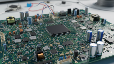
Understanding the basics of PCB design is crucial for anyone venturing into electronics. A printed circuit board (PCB) serves as the foundation for connecting various electronic components, providing both mechanical support and electrical pathways. The primary function of a PCB is to ensure that current flows between components such as resistors, capacitors, and integrated circuits, facilitating the performance of complex tasks within electronic devices.

Knowledge of circuit layouts, signal integrity, and the impact of label size and placement are fundamental components in crafting an effective PCB.

When starting the design process, it’s essential to grasp the fundamental types of PCBs, including single-sided, double-sided, and multilayer boards. Each variation offers distinct advantages in terms of complexity, size, and cost-effectiveness.

Furthermore, familiarizing oneself with design software tools can streamline the designing process, enabling easier manipulation of circuit paths and component placement. A well-thought-out design can reduce issues like interference and signal loss, which are critical for the board's overall reliability and performance.

Understanding these foundational concepts will provide a strong base as you embark on your PCB design journey.

Choosing the Right Software for PCB Design

When embarking on your journey to design your first PCB, the choice of software is crucial. With numerous options available, selecting the right platform can significantly impact your design efficiency and accuracy. Recent reports indicate that over 60% of PCB designers prioritize software usability and features when making their selection. This underscores the importance of finding a tool that not only meets your technical needs but also enhances your workflow.

As you explore your options, consider these tips:

  • First, familiarize yourself with the software's user interface and capabilities. Many software solutions provide trial versions, allowing you to assess their features without a hefty investment.
  • Second, ensure the software supports the necessary file formats for manufacturing, as compatibility is essential for a seamless transition from design to production.
  • Lastly, take advantage of community forums and resources associated with the software; these can provide valuable insights and troubleshooting assistance.

In addition to software features, it's vital to assess the level of technical support offered. A recent survey showed that 45% of engineers experienced project delays due to insufficient support from their PCB design software providers. Therefore, prioritize tools that come with robust customer service options, as this can save you time and frustration in the long run.

Guidelines for Creating an Effective Schematic Diagram

Creating an effective schematic diagram is a crucial step in designing your first PCB (Printed Circuit Board). A well-structured schematic not only simplifies the design process but also serves as a clear roadmap for your project. Begin by ensuring that all components are represented accurately, with their values and specifications clearly labeled. Using standardized symbols is essential for clarity, as it allows anyone viewing the schematic to quickly grasp the configuration without confusion.

Additionally, consider the layout of your schematic. Organizing components logically and using a grid can enhance readability and help in identifying connections easily. Group related components together, and use hierarchical structures if your design becomes complex. Properly managing the connections and minimizing crossing lines will reduce errors during the PCB layout phase. Lastly, always remember to annotate your schematic with any necessary notes or explanations. This level of detail fosters better communication with collaborators and aids in future troubleshooting.

Component Usage in PCB Design

This bar chart displays the frequency of different components used in PCB design, which is essential for understanding the design requirements and optimizing the layout of your printed circuit board.

Tips for Layout Optimization and Component Placement

When designing your first printed circuit board (PCB), layout optimization and component placement are crucial aspects to ensure functionality and performance. Start by sketching a rough layout of your circuit to visualize how components will interact. Group related components together to minimize trace lengths, which not only saves space but also reduces signal interference. Keep high-frequency pathways as short as possible, and remember to consider the flow of power and ground to avoid noise and grounding issues.

In addition to efficient organization, think about the physical arrangement of components. Place components that will be connected directly close together to facilitate easier soldering and reduce the risk of assembly errors. Use a hierarchical approach, organizing your PCB layout by function: for example, keep analog components separate from digital elements to reduce electromagnetic interference. Lastly, always leave room for heat dissipation; components that generate heat should be spaced appropriately to prevent performance degradation. With these tips in mind, you’ll be on your way to creating a well-optimized PCB layout that functions reliably.

Best Practices for Testing and Prototyping Your PCB Design

10 Essential Tips for Designing Your First PCB Printed Circuit Board

When designing your first printed circuit board (PCB), focusing on effective testing and prototyping is crucial to ensure functionality and reliability. Start with a robust prototype that allows you to assess your design in real-world scenarios. Utilize simulation software to identify potential issues before moving to the physical stage. This step can save time and resources by identifying flaws early, ensuring that your design behaves as expected under various conditions.

Once your prototype is ready, employ a systematic approach to testing. Begin with basic functionality tests to verify that the board powers up and all components function as intended. Gradually introduce more complex tests, such as stress testing and thermal evaluation, to observe how your PCB performs under different loads and environmental conditions. Documenting these tests provides valuable insights into the design's strengths and weaknesses, allowing for necessary adjustments before final production, ultimately enhancing the quality and longevity of your PCB design.