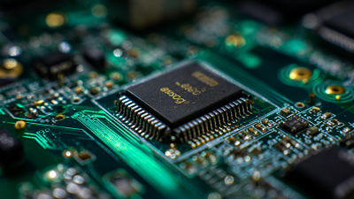
The Future of PCB Prototyping: Innovations Shaping Tomorrow's Electronics
As the electronics industry accelerates toward a more interconnected and technology-driven future, PCB prototyping stands at the forefront of innovation, shaping how devices are conceived and brought to market. According to a recent report by the IPC (Association Connecting Electronics Industries), the global PCB market is projected to reach $85 billion by 2026, driven by an increasing demand for miniaturization and enhanced functionality in consumer electronics. Moreover, the rapid evolution of technologies such as IoT, AI, and 5G is pushing the boundaries of what is possible in printed circuit board design and manufacturing. As we explore the future of PCB prototyping, it is essential to consider the cutting-edge advancements that are set to revolutionize the industry, streamline production processes, and ultimately impact the overall consumer experience.
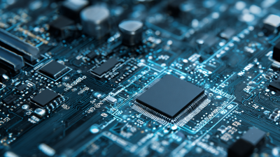
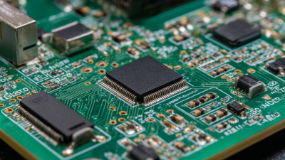
Emerging Technologies Transforming PCB Prototyping Processes
Emerging technologies are revolutionizing PCB prototyping processes, setting the stage for smarter and more efficient electronics manufacturing. According to a report by Research and Markets, the global PCB market is expected to reach $90 billion by 2025, driven largely by advancements in prototyping technologies. Innovations such as automated PCB assembly and advanced simulation tools are enhancing the speed and accuracy of prototype development, allowing companies to significantly decrease time-to-market.
For those looking to optimize their PCB prototyping efforts, consider investing in software that integrates AI and machine learning capabilities. These tools can streamline design processes, identify potential issues early, and enhance overall efficiency. Additionally, utilizing 3D printing for rapid prototyping grants unparalleled flexibility, enabling designers to quickly iterate and refine their concepts without the lead time associated with traditional manufacturing methods.
Keep an eye on multilayer PCBs and flexible circuits, as they are gaining popularity in advanced applications such as wearables and IoT devices. The ability to create densely packed, lightweight designs extends the functionality of products while reducing associated costs. By embracing these emerging technologies, companies can not only improve their prototyping processes but also stay ahead in a competitive market.
The Future of PCB Prototyping: Innovations Shaping Tomorrow's Electronics
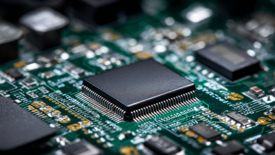
Key Innovations in Design Software for Efficient PCB Development
The future of PCB prototyping is being significantly shaped by innovations in design software, which are crucial for efficient PCB development. According to industry reports, the global PCB market is expected to grow to $78 billion by 2025, driven by advancements in technologies such as artificial intelligence and the Internet of Things. These technologies enable more sophisticated design capabilities, allowing engineers to optimize layouts and improve performance while reducing time to market.
Recent developments in bio-microsystem integration and Lab-on-PCB technology represent a breakthrough in the electronics manufacturing landscape. With the concept of micro-total analysis systems (µTAS) emerging in the early 1990s, the integration of laboratory functions onto a single chip has opened new avenues for medical diagnostics and environmental monitoring. Innovations in design software now streamline these complex integrations, making it easier for startups and established companies alike to exploit these cutting-edge technologies and deliver next-generation products that meet growing consumer and industrial demands.
The Future of PCB Prototyping: Innovations Shaping Tomorrow's Electronics
| Innovation |
Description |
Impact on PCB Development |
Expected Adoption Year |
| AI-Powered Design Tools |
Tools that utilize artificial intelligence to optimize design layouts. |
Reduces design time and enhances accuracy. |
2025 |
| Cloud-Based Collaboration Platforms |
Platforms enabling real-time collaboration among design teams across different locations. |
Facilitates faster feedback cycles and improves team productivity. |
2024 |
| 3D PCB Modeling |
Innovative modeling techniques that allow for 3D visualization of PCBs. |
Improves layout efficiency and helps identify potential issues early. |
2026 |
| Automated Error Checking |
Systems that automatically check for design errors in real-time. |
Minimizes the risk of costly design flaws. |
2025 |
| Flexible PCB Technology |
Technologies that enable the creation of flexible and stretchable PCBs. |
Expands design possibilities for wearable and portable devices. |
2027 |
Advancements in Materials: The Next Generation of Flexible PCBs
The advancement of materials in PCB prototyping is transforming the electronics landscape, particularly with the emergence of flexible printed circuit boards (FPCBs). According to a report by MarketsandMarkets, the flexible PCB market is projected to reach $36.1 billion by 2026, growing at a CAGR of 10.5% from 2021. This growth is driven by the increasing demand for miniaturized electronic devices and the need for lightweight, space-efficient designs. FPCBs are crucial for applications in consumer electronics, automotive, and medical devices, where adaptability and performance are paramount.
Recent innovations in materials, such as improved polymers and conductive inks, are enhancing the capability and flexibility of PCBs. Advanced materials like polyimide and high-density interconnect (HDI) are enabling FPCBs to withstand higher temperatures and more complex circuit designs. Furthermore, the integration of organic and inorganic materials is allowing for greater electrical performance and durability. As the industry evolves, companies that harness these advancements will be better positioned to meet the demands of next-generation electronics, setting a new standard in PCB prototyping and design.
Rapid Prototyping Techniques: Speeding Up Electronic Product Development
In the fast-evolving world of electronics, rapid prototyping techniques are revolutionizing the way products are developed. By leveraging advanced technologies such as 3D printing, laser cutting, and CNC machining, engineers can create prototypes in a fraction of the time it traditionally takes. This acceleration not only enhances creativity in design but also facilitates quicker iterations based on real-time feedback, allowing designers to refine their concepts before moving to mass production.
Tip: When starting a prototyping project, utilize digital twin technology to simulate your design and identify potential issues before physical fabrication. This proactive approach can save resources and reduce time spent on revisions.
Moreover, adopting agile methodologies within the prototyping phase enables teams to respond swiftly to market changes and customer feedback. Shorter development cycles lead to a more streamlined process, ensuring that innovative products reach consumers faster than ever.
Tip: Embrace collaboration tools and platforms that allow team members to share ideas and revisions instantly. This continuous communication loop fosters an environment of creativity and swift problem-solving throughout the prototyping phase.
Sustainability in PCB Manufacturing: Eco-Friendly Practices for the Future
In today's rapidly evolving electronics landscape, sustainability is becoming a crucial consideration in PCB manufacturing. As environmental concerns intensify, manufacturers are embracing eco-friendly practices that not only minimize waste but also ensure the longevity of materials used in production. This shift towards green PCB prototyping involves the use of recyclable materials and non-toxic substances, significantly reducing the environmental footprint of electronic devices. By implementing efficient waste management systems and opting for renewable resources, companies are not only contributing to environmental preservation but also aligning with the growing consumer demand for sustainable products.
Moreover, advancements in technology are paving the way for innovative manufacturing processes that enhance sustainability in PCB production. Techniques such as additive manufacturing and laser direct imaging are revolutionizing traditional methods, allowing for more precise and less wasteful production. These innovations not only streamline the manufacturing process but also support the creation of more compact and efficient designs, which can reduce energy consumption throughout the product lifespan. As the industry continues to prioritize sustainability, the future of PCB prototyping will undoubtedly reflect a commitment to eco-friendly practices, shaping a healthier planet for generations to come.