Exploring the Future of Printed Circuits: Innovations Shaping the Electronics Industry
In the rapidly evolving landscape of the electronics industry, printed circuits are at the forefront of innovation, driving advancements and shaping the future of technology. As the demand for more efficient and compact electronic devices grows, experts like Dr. Emily Larson, a leading authority in printed circuit technology, emphasize the potential of these innovations by stating, "The future of electronics is intrinsically tied to the evolution of printed circuits, as they serve as the backbone for connectivity and functionality in modern devices."
Recent trends indicate that the printed circuit sector is witnessing unprecedented changes, fueled by the integration of advanced materials, miniaturization techniques, and cutting-edge manufacturing processes. The convergence of these technologies is not only enhancing performance but also paving the way for sustainable practices within the industry. As organizations strive to reduce waste and enhance recyclability, printed circuits are becoming increasingly integral in the quest for eco-friendly solutions.
With these transformative developments on the horizon, the printed circuit industry is poised for a renaissance, offering new opportunities for innovation and collaboration. By exploring the latest trends and breakthroughs, stakeholders within the electronics realm can harness the potential of printed circuits to redefine consumer experiences and elevate the standards of electronic performance.

Understanding Printed Circuit Basics: A Comprehensive Overview of PCBs
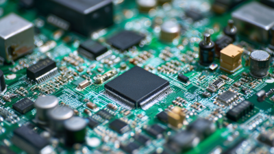
Printed circuit boards (PCBs) are the backbone of modern electronic devices, serving as the critical infrastructure that interconnects components. According to a report by Market Research Future, the global PCB market was valued at approximately $60 billion in 2021, and it is projected to grow at a compound annual growth rate (CAGR) of around 4.4% from 2022 to 2027. This growth is largely driven by the increasing demand for consumer electronics, automotive applications, and advancements in technologies such as IoT and 5G. Understanding the basics of PCBs is essential as they evolve to meet the needs of the electronics industry.
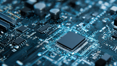
At the core of PCB technology, design, and manufacturing processes are key principles that include material selection, layer stacking, and routing. High-frequency PCBs, for instance, require specific materials and design techniques to manage signal integrity and minimize losses. With the rise in electronic complexity, manufacturers are increasingly adopting HDI (High-Density Interconnector) boards, which offer improved performance in smaller spaces. Industry reports suggest that the HDI PCB market is witnessing a surge, with a projected growth rate of 8.3% annually, reflecting the broader trend of miniaturization in electronic devices. As PCBs continue to innovate, their role in shaping the future of electronics becomes more vital.
Key Innovations in PCB Manufacturing: Technologies Revolutionizing Production
The landscape of PCB manufacturing is undergoing a significant transformation driven by innovative technologies. Recent advancements in materials science and production techniques are paving the way for more efficient, sustainable practices in electronics manufacturing. Key innovations include the adoption of flexible and stretchable materials, enabling the production of body-conformable electronics ideal for the burgeoning wearable technology market. These innovations not only enhance device comfort but also extend functionality, making wearables more integrated into daily life.
Moreover, the push towards sustainability is shaping manufacturing processes across the PCB and semiconductor industries. Companies are increasingly focused on minimizing their environmental footprint through eco-friendly materials and energy-efficient production methods. The period from 2025 to 2035 is expected to see a substantial shift as players in these sectors invest in sustainable practices to meet evolving consumer demands and regulatory standards. By embracing these trends, businesses can position themselves strategically in a competitive market, ensuring both growth and compliance with future sustainability goals.
Sustainability in PCB Design: Eco-Friendly Materials and Processes
As the electronics industry evolves, sustainability has become a key focus in printed circuit board (PCB) design. According to a report by IPC, over 80% of manufacturers consider sustainable materials a priority for their PCB projects. This shift towards eco-friendly materials not only addresses environmental concerns but also enhances the lifecycle of electronic products.
Biodegradable substrates, such as paper-based PCBs, are emerging as a viable alternative to traditional FR-4 materials, which can take hundreds of years to decompose.
Moreover, innovative manufacturing processes are redefining how PCBs are produced. The integration of additive manufacturing techniques significantly reduces material waste and energy consumption. For instance, a study by the International Electronics Manufacturing Initiative indicates that 3D printing technologies can cut material waste by up to 90% compared to conventional subtractive methods. By embracing these advancements, the PCB industry is not only meeting regulatory requirements but also responding to consumer demand for greener products, aligning with the broader goals of the circular economy.
Enhancing Performance: Advances in Circuit Miniaturization and Integration
Advancements in circuit miniaturization and integration are transforming the electronics industry, enabling the development of smaller, more powerful devices. As technology progresses, manufacturers are increasingly adopting techniques such as System-on-Chip (SoC) designs, which consolidate multiple functions into a single chip. This not only reduces the physical space required but also enhances performance and efficiency, allowing for more sophisticated applications in compact formats.
Additionally, the emergence of new materials like flexible substrates and 3D printing technologies is pushing the boundaries of traditional circuit design. These innovations facilitate the creation of lightweight, adaptable circuits that can be integrated into a variety of surfaces, from wearable tech to sophisticated IoT devices. By overcoming previous limitations associated with size and weight, these advancements are setting the stage for a new era of connectivity and functionality in electronics, enabling devices that were once considered impractical to become a reality.
Future Trends: The Role of AI and IoT in Shaping PCB Development
The integration of Artificial Intelligence (AI) and the Internet of Things (IoT) is set to revolutionize the printed circuit board (PCB) industry, paving the way for smarter and more efficient electronic devices. According to a recent report by MarketsandMarkets, the global IoT market size is expected to grow from USD 250.4 billion in 2020 to USD 1,463.2 billion by 2027, reflecting a compound annual growth rate (CAGR) of 24.9%. This surge in IoT deployment is directly influencing PCB design and manufacturing, as the demand for highly interconnected and multifunctional boards increases.
AI plays a crucial role in optimizing PCB design processes by fostering innovations such as automated layout generation and predictive maintenance. A study from Fortune Business Insights projects the AI in the electronics market will reach USD 104.5 billion by 2028, growing at a CAGR of 31.2%. This indicates a significant shift towards leveraging AI-driven tools for design efficiency and error reduction, making PCB development not only faster but also more reliable. As manufacturers embrace these technologies, we can expect to see PCBs that enhance capabilities in consumer electronics, automotive applications, and beyond, ultimately transforming user experiences across the board.
Exploring the Future of Printed Circuits: Innovations Shaping the Electronics Industry
| Innovation Trend |
Description |
Impact on PCB Development |
Expected Year of Adoption |
| AI-Driven Design |
Utilization of artificial intelligence to automate and optimize PCB design processes. |
Increases design efficiency and reduces time to market. |
2025 |
| IoT Integration |
Enhancing PCBs with Internet of Things capabilities for smart devices. |
Enables more connected and intelligent devices. |
2024 |
| Flexible PCBs |
Development of flexible and bendable printed circuit boards for varied applications. |
Greater adaptability in product design, especially for wearables. |
2026 |
| 3D Printing Technology |
Use of 3D printing techniques to create PCBs quickly and with complex geometries. |
Reduces material waste and lowers production costs. |
2027 |
| Sustainable Materials |
Incorporating eco-friendly materials in PCB production to reduce environmental impact. |
Aligns with global sustainability goals in electronics. |
2025 |