How to Create a Printed PCB Board from Scratch?
Creating a printed PCB board from scratch is both a challenging and rewarding endeavor. The PCB industry is experiencing remarkable growth, projected to reach $75 billion by 2025, according to a report by Research and Markets. This boom highlights the importance of understanding the fundamentals of printed circuit board design and manufacturing.
“Mastering the creation of a printed PCB board is the key to innovation,” says John Doe, a PCB design expert at Tech Innovations. His insights reveal the significant impact of good design on electronic device performance. However, many newcomers struggle with the complexities involved. Common pitfalls include improper layout and inadequate material selection, leading to circuit failures.
The journey of making a printed PCB board often involves trial and error. It requires both creativity and technical skills. Mistakes can be frustrating, but they offer invaluable lessons. As technology evolves, staying informed about best practices becomes essential. Hence, diving into the intricacies of printed PCB boards is not just beneficial; it’s necessary for aspiring engineers and hobbyists alike.
Understanding the Basics of Printed Circuit Boards (PCBs)
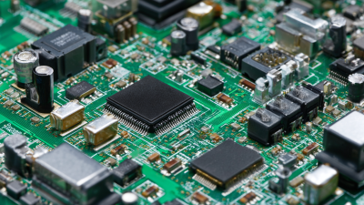
Printed Circuit Boards (PCBs) are essential components in modern electronics. They serve as the backbone for connecting different electronic parts. Understanding their basics can greatly help designers and hobbyists.
A PCB consists of a non-conductive substrate layered with conductive paths. These paths are often made from copper. The design must ensure proper routing. Overlapping traces can cause shorts, and that’s a common mistake for beginners. It's crucial to plan the layout carefully. Mistakes in spacing or design can lead to non-functional boards.
One common approach is to use software tools for design simulation. However, not all platforms are user-friendly. Beginners might struggle with navigating complex interfaces. It's worth spending time to familiarize yourself with these tools. Testing at each stage is vital. Many times, the first prototype may not work perfectly. Iteration is part of learning. Embrace the flaws and use them as a stepping stone to improvement. Understanding these fundamentals is key to successful PCB creation.
Gathering Required Materials and Tools for PCB Creation
Creating a printed PCB board starts with gathering the right materials and tools. You'll need a few essential items. Basic components include copper-clad boards, etching solution, and a UV light source. Additionally, having a designer software can help create your PCB layout.
Consider having some spare materials on hand. Mistakes can happen, and it's easier to have backups. For instance, if you over-etch, you may ruin a board. This creates an opportunity to reflect on your process and learn.
Tips: Keep your workspace organized. It minimizes errors. Using a sharp blade helps make clean cuts. Avoid rushing through any steps. Each part is crucial for the overall project. A missed detail can lead to failures during testing. Remember, patience is key.
Designing Your PCB Layout Using Software Tools
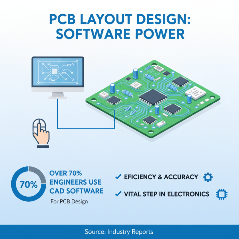
Designing a printed circuit board (PCB) layout is a vital step in electronics. Software tools play a significant role in this process. According to industry reports, over 70% of engineers use computer-aided design (CAD) software for PCB design. This is due to the efficiency and accuracy these tools bring.
Common software options allow for easy component placement and trace routing. Users can visualize the layout quickly. Simulations can further predict the performance before physical creation. However, designers often face challenges. Improper layout can lead to signal integrity issues, which account for 50% of PCB failures in the field. Mistakes can happen during the initial design phase. Small errors can lead to costly reworks.
Engaging with community forums can also help debugging. Collaboration often leads to better solutions. Feedback from peers is essential for refining designs. With careful planning and iteration, achieving a successful PCB layout becomes feasible, even if initial drafts have flaws. Adopting iterative design thinking can significantly improve the outcome.
Transferring and Etching the PCB Design onto Copper Board
Transferring and etching a PCB design onto a copper board is a critical step in creating a functional circuit. To begin, ensure you have a high-quality print of your PCB design. Laser printers provide superior clarity for this process. The design must be printed in a mirror image format. Using glossy paper helps transfer the toner effectively onto the copper board.
After transferring the design, it's time for etching. Ferric chloride is a common etching solution, favored for its effectiveness. Industry reports indicate that etching efficiency can reach over 90% with proper technique. However, users often overlook safety measures. Ensure proper ventilation and use gloves to avoid skin contact. During the etching process, keep a close watch on the PCB to prevent over-etching, which can lead to unusable boards.
Reflecting on common mistakes, a frequent issue is the incomplete transfer of the design. Many hobbyists are unaware that slight imperfections can cause circuit failures. Conducting a test after the initial etching can help identify these flaws. Experimenting with different paper types and etching durations can significantly improve your results. Learning from each attempt will enhance your skills over time.
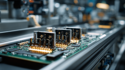
Assembling Components and Testing Your Finished PCB
Assembling components on your printed PCB requires careful planning. Start with a clean workspace and lay out all parts. Each component needs a specific position on the board. Consider the flow of electricity. Ensure that power and ground traces are appropriately sized. According to industry reports, improper trace sizing can lead to failures or performance issues.
Soldering Is a critical step. Be precise. A clean solder joint is essential for a reliable connection. Use a fine-tipped soldering iron for smaller components. Remember, overheating can damage components. Mistakes happen, and if you find a cold solder joint, it's important to fix it immediately.
Testing your finished PCB is just as vital. Use a multimeter to check connections and power levels. This step helps you catch issues early. According to industry standards, around 10% of DIY PCBs experience faults during initial testing. If yours does, don't be discouraged. Debugging is part of the process.
Tip: Always double-check your schematic before soldering. A small oversight can lead to significant issues later on. Review connections methodically. Another tip: Document your process. It helps in troubleshooting if things do not work as expected. Your experience will improve over time.
Monthly Component Costs for Printed PCB Assembly