Exploring Innovative Alternatives for Best PCB Fabrication Assembly in Global Manufacturing
In the rapidly evolving landscape of global manufacturing, the demand for advanced technology solutions has never been greater, particularly in the realm of PCB fabrication assembly. According to a recent report by MarketsandMarkets, the printed circuit board (PCB) market is projected to reach $104.4 billion by 2026, driven by the proliferation of electronics across industries such as automotive, healthcare, and telecommunications. As manufacturers seek to optimize production efficiency and minimize costs, exploring innovative alternatives in PCB fabrication assembly becomes crucial. This blog will delve into various cutting-edge techniques and materials that not only enhance manufacturing processes but also align with sustainability goals, ensuring that businesses remain competitive in an increasingly complex market. By harnessing innovative technologies and methodologies, manufacturers can achieve superior quality, faster turnaround times, and higher flexibility in their PCB fabrication assembly processes.
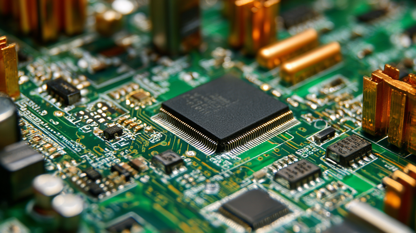
Understanding PCB Fabrication: Key Technical Parameters You Need to Know
In the realm of PCB (Printed Circuit Board) fabrication, understanding key technical parameters is crucial for achieving optimal assembly outcomes. Initially, one must consider the substrate material, which significantly impacts the board's performance and durability. Common substrates, such as FR-4, provide excellent electrical insulation but may not suffice for high-frequency applications where materials like Rogers or Teflon are preferred. The choice of substrate directly influences thermal conductivity and dielectric properties, making it essential to align material selection with the intended application.
Another vital parameter is layer count, which determines the PCB's compactness and complexity. Multi-layer PCBs enable more intricate designs and denser circuit arrangements, enhancing functionality while promoting efficient use of space. However, with increased layers comes the challenge of managing impedance control and signal integrity. Additionally, copper thickness is a critical aspect that affects current carrying capacity and the overall reliability of the PCB. Selecting the appropriate thickness is essential for meeting both operational demands and manufacturing standards, ensuring that the final product can withstand the rigors of real-world applications. Understanding these parameters facilitates informed decision-making in PCB fabrication, setting the stage for innovation and quality in global manufacturing.
Innovative Materials in PCB Assembly: Advancements and Benefits
Innovative materials play a crucial role in the advancement of PCB assembly, significantly impacting the efficiency and performance of electronic devices. Recent developments in lightweight composite structures have been transformative, offering enhanced durability and reduced weight for PCBs. These materials not only improve the overall functionality of electronic products but also align with the industry's growing emphasis on sustainability and energy efficiency. As these innovations continue to evolve, they provide manufacturers with the opportunity to create more cost-effective and eco-friendly solutions.
Moreover, the rising capabilities of countries like China and India in advanced manufacturing highlight a shift in global dynamics. China's advancements in innovation are reflected in its universities and domestic companies, pushing the boundaries of materials used in PCB assembly. Similarly, India's growing role in global trade competitiveness showcases its potential to contribute to innovative manufacturing processes. As these nations harness new technologies and materials, they not only enhance their production capabilities but also position themselves as leaders in the rapidly changing landscape of global PCB fabrication.
Step-by-Step Guide to Optimizing PCB Fabrication Processes
Optimizing PCB fabrication processes is crucial for enhancing efficiency and reducing costs in global manufacturing. The first step in this journey is to evaluate your current processes meticulously. Identify bottlenecks that slow down production, such as long lead times for materials or inefficient routing within the assembly line. Implementing Lean principles can streamline workflows by minimizing waste and improving overall productivity, ultimately leading to faster delivery times and enhanced customer satisfaction.
Once bottlenecks are addressed, integrating advanced technologies can significantly elevate the fabrication process. Automation, for instance, can improve precision and consistency in soldering and component placement. Additionally, incorporating data analytics allows manufacturers to monitor production metrics in real-time, enabling quicker decisions based on actionable insights. By leveraging these technologies, companies can not only optimize their existing processes but also innovate new methods to stay ahead in a competitive market.
Global Trends in PCB Manufacturing: What You Should Be Aware Of
In the rapidly evolving landscape of global manufacturing, understanding the latest trends in PCB (Printed Circuit Board) manufacturing is crucial for companies looking to stay competitive. One significant trend is the increasing push towards automation and smart factories. Manufacturers are incorporating advanced robotics and AI technologies to streamline their assembly lines, enhance precision, and reduce costs. This shift not only improves efficiency but also allows for greater customization, enabling companies to quickly adapt to changing market demands.
Another notable trend is the growing emphasis on sustainability within the PCB industry. With environmental concerns at the forefront, many manufacturers are exploring eco-friendly materials and processes. Innovations in waste reduction, energy-efficient production techniques, and the use of recyclable materials are gaining traction. Companies that prioritize sustainability are not only fulfilling regulatory requirements but also appealing to a more eco-conscious consumer base, which can lead to enhanced brand loyalty and market differentiation. As the industry continues to evolve, staying informed about these trends will be essential for making informed decisions in PCB fabrication and assembly.
Troubleshooting Common Issues in PCB Assembly: Tips and Techniques
In the realm of PCB assembly, troubleshooting common issues is vital for maintaining production efficiency and ensuring product quality. One pressing challenge in this field is the effectiveness of solder mask repairs. When dealing with defective PCBs, understanding proper solder mask repair techniques can help restore functional capability without necessarily meeting original specifications. This approach allows manufacturers to adopt repair-oriented design strategies that cater to the evolving demands for sustainability and efficiency in electronic production.
To further enhance troubleshooting, here are a few helpful tips: First, always examine the solder joints closely; proper inspection can identify potential issues before they escalate. Second, leverage machine vision technology; integrating AI in quality control processes can expedite inspection and improve accuracy, ensuring defects are caught early in the assembly line. Finally, maintain thorough documentation of past repairs and adjustments, as this data can provide valuable insights into recurring problems and guide future troubleshooting efforts. These practices not only streamline operations but align with the growing need for sustainable and repairable electronic manufacturing.
Trends in PCB Assembly Issues and Solutions (2023)
This chart depicts the most common issues faced during PCB assembly along with effective solutions adopted by manufacturers over the past year.