Essential Steps in PCB Prototyping: A Comprehensive Guide for Beginners
In the fast-evolving world of electronics, PCB prototyping stands as a crucial step for designers and engineers aiming to transform their ideas into tangible products. Whether you are a novice or just looking to refine your skills, understanding the essential steps in PCB prototyping is fundamental to ensuring that your designs function correctly and efficiently. This comprehensive guide will walk you through the entire process, from initial design considerations and software selection to fabrication and testing. By breaking down these complex stages into manageable tasks, we aim to empower beginners with the knowledge and confidence needed to embark on their PCB prototyping journey. Embracing this foundational skill not only enhances your project outcomes but also lays the groundwork for future innovation and creativity in electronics.

Understanding the Basics of PCB Prototyping for Beginners
 PCB prototyping is a crucial step in the development of electronic devices, offering a way for beginners to turn their concepts into tangible products. Understanding the basics of this process is vital; it encapsulates the journey from design to production. According to the market research report from Mordor Intelligence, the global PCB prototyping market is projected to grow at a CAGR of 6.2% from 2021 to 2026. This growth highlights the increasing reliance on rapid prototyping techniques, enabling faster iteration and development cycles for new electronic products.
For beginners, grasping essential concepts like design software, materials, and fabrication techniques is vital. Software tools such as Eagle and Altium are pivotal in creating PCB layouts, ensuring that connections are both efficient and reliable. Furthermore, insights from Research and Markets emphasize that the adoption of 3D printing in PCB prototyping is reshaping the industry, allowing for quicker and more cost-effective production of complex designs, thereby making it more accessible for newcomers. This evolving landscape emphasizes the importance of staying updated on trends and technologies to enhance prototyping skills and efficiency.
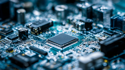
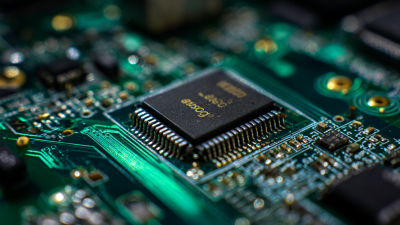
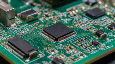
Essential Tools and Equipment Needed for PCB Prototyping
When venturing into PCB prototyping, having the right tools and equipment is crucial for success. A basic toolkit should include a high-quality soldering iron, essential for making reliable connections between components on the board. Look for a temperature-controlled iron, as this allows for precision when working with delicate components. Additionally, a multimeter is indispensable for testing circuits and ensuring that everything functions correctly before the final assembly.
Another essential piece of equipment is a PCB design software. Many beginners might feel overwhelmed by the options available, but programs like Eagle or KiCAD offer user-friendly interfaces that make the design process more intuitive. Beyond software, a good set of wire strippers, pliers, and tweezers will help in assembling components neatly and efficiently. Furthermore, investing in a proper workspace with adequate lighting and an anti-static mat can significantly enhance your prototyping experience, ensuring both safety and precision as you bring your electronic ideas to life.
Essential Tools and Equipment Needed for PCB Prototyping
Step-by-Step Process of Designing Your First PCB Prototype
Embarking on your first PCB prototyping journey can be both exciting and daunting. This step-by-step guide will help you navigate through the essential stages of designing a printed circuit board. Start by defining the purpose of your PCB and outlining its requirements. This initial planning phase is critical, as it sets the foundation for the entire design process. Take time to sketch your circuit diagram, ensuring all components and connections are clearly represented.
Tip: Utilize software tools like KiCad or Eagle to create your schematic. These programs can simplify the design process and minimize errors, especially for beginners.
Once your schematic is ready, follow up with the layout design. Place components on the board, ensuring optimal spacing and routing of traces for efficient electrical flow. Pay attention to design rules regarding trace width and clearance, as they can impact the performance of your PCB.
Tip: Don’t hesitate to iterate on your layout. Making adjustments early can save you time and resources in the prototyping stage. Remember to run a design rule check (DRC) to identify any potential issues before fabrication.
Common Challenges in PCB Prototyping and How to Overcome Them
PCB prototyping is an essential phase in electronics design, but it comes with its own set of challenges. As the demand for smaller, more complex devices increases, engineers often struggle to fit more components onto compact printed circuit boards (PCBs). Recent trends in flexible PCB technology provide viable solutions by allowing engineers to design layouts that adapt to smaller form factors, thus simplifying the integration of multiple components.
To navigate common challenges in PCB prototyping such as layout complexity and component density, here are some useful tips. First, consider utilizing modern CAD tools that support both electronic and mechanical designs; this integration can streamline workflows and minimize errors. A unified environment can help validate designs early in the process, reducing the risk of costly revisions. Second, leverage simulation software to analyze potential design challenges early, particularly when working with high-speed interconnects, which are becoming increasingly complex. This proactive approach can save time and resources later in the prototyping phase.
Lastly, be mindful of the intricacies involved in testing complex PCB assemblies. As circuit board designs grow in complexity, effective testing strategies become paramount to ensure reliability and performance. Emphasizing rigorous testing protocols can help overcome potential pitfalls, ensuring a successful transition from prototype to production.

Testing and Evaluating Your PCB Prototype: Best Practices
When it comes to testing and evaluating your PCB prototype, implementing best practices is essential for ensuring functionality and reliability. Start by conducting thorough electrochemical analysis, especially if your PCB plays a role in energy storage applications such as supercapacitors. Understanding the specific electrochemical responses of the components can reveal potential pitfalls early in the development process. This iterative testing approach helps streamline further iterations and optimizes design modifications.
Tip 1: Always perform cleanliness tests, like the resistivity of solvent extract (ROSE) testing, to evaluate surface contaminants that could affect the PCB's performance. Ensuring a clean prototype is crucial for reliable electrical connections and overall operation.
Additionally, consider exploring innovative encapsulation methods to protect your PCB. Using biocompatible materials for encapsulation not only safeguards the circuits from environmental damage but also ensures compliance with safety standards. This is especially important in applications where the PCB may be subject to harsh conditions or in healthcare-related products.
Tip 2: Always document your testing procedures and results meticulously. This practice helps in troubleshooting and refining your prototype based on empirical data, leading to a more robust final product that meets your design specifications.
Essential Steps in PCB Prototyping: A Comprehensive Guide for Beginners
| Step |
Description |
Best Practices |
Testing Method |
Evaluation Criteria |
| 1. Design |
Create a schematic design using CAD software. |
Ensure all components are correctly placed and connections are valid. |
Simulation Testing |
Functionality matches the intended design. |
| 2. Prototype Fabrication |
Manufacture the designed PCB using appropriate methods. |
Choose reliable fabrication services. |
Visual Inspection |
Physical integrity and solder quality. |
| 3. Assembly |
Assemble the components onto the PCB. |
Follow the component placement guide accurately. |
Functional Testing |
All components should be placed and soldered correctly. |
| 4. Functionality Test |
Test the PCB’s performance under operational conditions. |
Use appropriate testing equipment and conditions. |
Load Testing |
Voltage and current levels meet specified requirements. |
| 5. Iteration |
Analyze test results and make necessary adjustments. |
Document changes and retest as needed. |
Comparison Testing |
Confirm improvements and functionality stability. |