Understanding the Role of PCB and Assembly in Modern Electronics: A Comprehensive Guide
In today's fast-paced technological environment, the significance of PCB and assembly in the realm of modern electronics cannot be overstated. As the backbone of electronic devices, printed circuit boards (PCBs) play a pivotal role in ensuring the functional integrity and reliability of various applications, from consumer gadgets to advanced industrial systems. The assembly process, which involves integrating electronic components onto the PCB, is equally crucial, as it impacts the overall performance, durability, and cost-effectiveness of the final product. This comprehensive guide aims to shed light on the intricate relationship between PCB and assembly, exploring their vital functions, the latest advancements in manufacturing techniques, and best practices for achieving optimal results. By understanding these elements, engineers and manufacturers can navigate the complexities of electronic design and production, ultimately leading to innovative solutions that meet the demands of an ever-evolving market.
The Significance of PCBs in Today's Electronic Devices
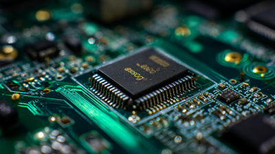
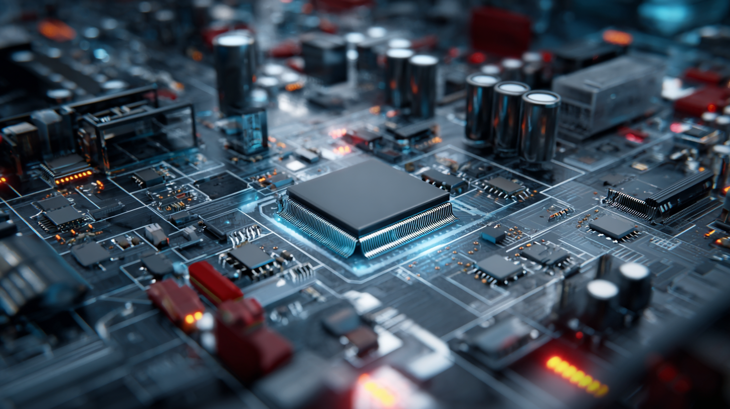
 Printed Circuit Boards (PCBs) are the backbone of modern electronic devices, serving as the foundational platform where electronic components communicate and function effectively. Their significance in today's electronics cannot be overstated; they provide mechanical support, electrical connectivity, and crucial signal integrity that dictate the performance and reliability of devices, from smartphones to complex industrial machines. Each PCB design must cater to the specific requirements of the device, emphasizing the need for precision in layout and material selection.
Tip: When designing a PCB, consider using a software tool that allows for real-time simulation and analysis. This can help in identifying potential issues early in the design process, saving time and resources.
Moreover, the assembly process of these PCBs is equally critical. The accuracy with which components are placed and soldered to the board directly influences the functionality and durability of the electronic device. Involving automated techniques alongside skilled workforce can enhance both efficiency and quality, ensuring that each device meets stringent industry standards.
Tip: Always conduct thorough testing on your PCBs post-assembly. Implementing techniques like Automated Optical Inspection (AOI) and functional testing can help catch defects that could lead to failures down the line.
Key Materials Used in PCB Manufacturing and Their Properties
In the realm of modern electronics, the choice of materials used in PCB manufacturing plays a crucial role in determining the performance, reliability, and cost-effectiveness of electronic devices. Key materials such as FR-4, a glass-reinforced epoxy laminate, dominate the market due to their excellent electrical insulating properties and mechanical strength. According to a report by MarketsandMarkets, the global FR-4 market is projected to reach $5.6 billion by 2025, reflecting its ubiquitous presence in consumer electronics, telecommunications, and automotive sectors.
Moreover, other materials like polyimide are gaining traction for high-temperature applications. Polyimide PCBs are known for their thermal stability and can withstand environments exceeding 200°C. The market for polyimide materials in PCB production is expected to grow significantly, with Research and Markets forecasting a compound annual growth rate (CAGR) of 5.9% from 2022 to 2027. This trend emphasizes the industry's shift towards materials that can endure harsher conditions, ensuring longevity and performance in critical applications, including aerospace and medical devices.
Understanding Key Materials Used in PCB Manufacturing
The Assembly Process: Techniques for Efficient Electronics Integration
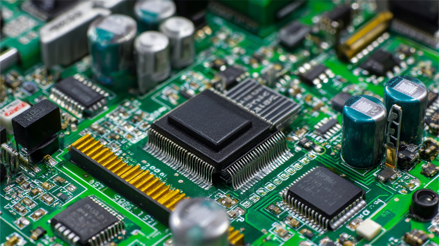
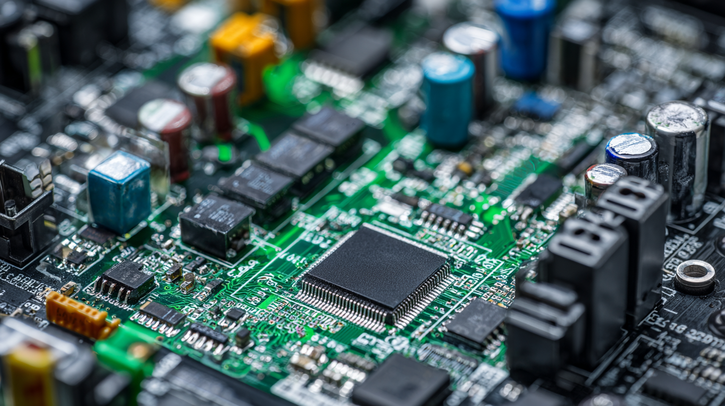
The assembly process is a critical phase in the production of modern electronics, requiring a blend of precision, innovation, and efficiency. Techniques such as surface mount technology (SMT) have revolutionized how components are integrated onto printed circuit boards (PCBs). SMT allows for components to be placed directly onto the surface of PCBs, reducing the space needed for circuit design and enhancing overall performance. This method not only speeds up the assembly process but also accommodates a higher component density, which is essential for miniaturized electronic devices.
Another significant technique in the assembly process is Through-Hole Technology (THT), which offers robust connections for components with larger leads. This method is particularly advantageous for applications requiring durability and mechanical strength, such as automotive electronics. Combining both SMT and THT in a single design can lead to optimal functionality, catering to the specific demands of various electronic products. By employing advanced automation and quality control measures throughout the assembly process, manufacturers can ensure high reliability and performance in their electronics, making this integration phase a cornerstone of modern technological innovation.
Understanding the Role of PCB and Assembly in Modern Electronics: A Comprehensive Guide
| PCB Type |
Material |
Layer Count |
Assembly Technique |
Lead Type |
| Rigid PCB |
FR-4 |
4 |
Surface Mount Technology (SMT) |
Lead-Free |
| Flexible PCB |
Polyimide |
2 |
Through-Hole Technology (THT) |
Lead |
| Rigid-Flex PCB |
FR-4 & Polyimide |
6 |
Mixed Technology |
Lead-Free |
| High-Frequency PCB |
PTFE |
4 |
SMT and THT |
Lead-Free |
Challenges in PCB Design and Assembly in Modern Applications
In the ever-evolving landscape of modern electronics, the design and assembly of printed circuit boards (PCBs) present a myriad of challenges that engineers must navigate. One significant hurdle is miniaturization, which has driven the need for more compact components and tighter tolerances. As devices become smaller and more complex, maintaining signal integrity while managing thermal dissipation becomes increasingly difficult. Engineers must employ advanced techniques and materials to ensure that PCBs can support high frequencies and meet the rigorous performance standards of today’s applications.
Additionally, the integration of IoT devices and smart technologies introduces further complexities into PCB design. Increased functionality often requires multi-layer boards, which complicate the assembly process. Ensuring reliability across varying environmental conditions adds another layer of challenge, necessitating thorough testing and validation procedures.
Furthermore, supply chain disruptions can lead to component shortages, forcing designers to adapt quickly by seeking alternative materials or redesigning to accommodate substitutions. As a result, an understanding of these challenges is crucial for anyone involved in PCB design and assembly to ensure the successful production of reliable and efficient electronic devices.
Future Trends in PCB and Assembly Technologies for Electronics
The landscape of PCB and assembly technologies is rapidly evolving, driven by the increasing demand for miniaturization and enhanced performance in modern electronics. One of the most significant trends is the rise of high-density interconnect (HDI) PCBs, which allow for more complex circuitry in a compact form. This technology supports the development of smaller devices without compromising functionality, making it ideal for applications in smartphones, wearable technology, and IoT devices. As manufacturers adopt automated assembly processes, precision and speed are improving, further enhancing production efficiency.
Another noteworthy trend is the integration of sustainable practices in PCB manufacturing and assembly. Companies are increasingly focused on reducing their environmental footprint by utilizing eco-friendly materials and processes. Biodegradable substrates and lead-free soldering techniques are gaining traction, aligning with global sustainability goals. Additionally, advanced manufacturing technologies such as 3D printing are beginning to play a crucial role in prototyping and creating on-demand components, allowing for greater customization and rapid iteration in design. Together, these advancements signal a transformative era in PCB and assembly technologies, paving the way for innovative electronic solutions.