WORLD electronics offers a complete line of electronic circuit board manufacturing and assembly services, as well as advanced manufacturing services. Our commitment to quality and service is second to no supplier.
Learn MoreOur team of engineers assists you in the development of new designs to optimize quality manufacturability (DFM) and testability, resulting in cost minimization and reduced product development time.
Learn MoreOur flexible manufacturing floor layout and highly trained staff allow for Quick Set-up and Tear Down of small volume prototype runs. This combination grants our customers the benefit of turning new designs quickly and accurately.
Learn MoreWORLD electronics is dedicated to quality. This quality is what underpins our commitment to thorough testing. Our engineers can develop a set of tests that ensure reliability and high performance in all products.
Learn MoreSupply chain management has crossed over from being a narrow management function to being a key operational function.
Learn MoreFlexible printed circuit boards are moving from specialized components into everyday product design. They carry signals through tight spaces while bending around hinges, curved housings, and moving assemblies. In a compact device, a thin flex circuit can replace several wires and connectors. That saves space, but it also makes material choice, bend radius, and assembly quality more consequential.
Market forecasts suggest continued interest. Grand View Research’s Flexible Printed Circuit Board Market Size, Share & Trends Analysis Report estimates a market value of USD 20.8 billion in 2023 and projects a 10.1% compound annual growth rate from 2024 to 2030. These are estimates, not guarantees; market figures can differ with research scope and definitions. Still, the direction is clear enough to merit a closer look.
This guide compares the main types expected to matter in 2026: single-sided, double-sided, multilayer, rigid-flex, and specialized flex circuits. Each serves a different design problem. A single-sided circuit may suit a simple camera module, while rigid-flex can connect boards across a folded product enclosure. The best choice depends on electrical demands, available space, expected movement, and production volume—not on flexibility alone.
That classification is useful, but not perfect. Some designs combine structures or use unusual materials, so labels can obscure important engineering differences. We will examine their construction, common applications, advantages, and trade-offs, using established industry terminology and practical design considerations. The goal is a clearer starting point for comparing options, not a substitute for qualified engineering review.
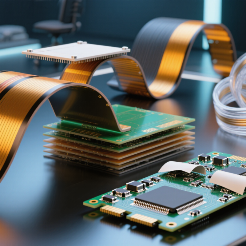
Single-sided flexible printed circuit boards carry copper traces on one side of a flexible insulating film, often polyimide. Their straightforward construction can reduce material use and make routing easier to inspect. A typical stack includes copper, a flexible base film, and a protective coverlay with openings at connection pads. These boards suit lightweight connections in sensor leads, display links, and compact control panels. Fewer layers do not mean carefree design. Trace width, copper thickness, bend radius, and connector reinforcement still matter.
A single-sided board works best when signals can travel without crossing. Component placement and shaped routes can help, while jumpers may add assembly steps. Consider how the board will bend: a one-time fold during installation creates different stress from repeated movement. Keep copper away from sharp corners, and confirm the bend zone with the fabricator. Small layout choices can affect long-term reliability.
Tips: Mark the bend area clearly. Keep components and solder joints outside it. Ask about minimum bend radius and copper details before release. Review a physical sample, too; drawings can hide awkward handling. Sometimes a prototype feels stiffer than expected.

Double-sided flexible printed circuit boards carry copper traces on both sides of a thin insulating film. Plated vias connect the layers, allowing more signals to fit into a compact assembly. This suits camera modules, wearable devices, and other products where a rigid board would crowd the enclosure. In practice, a folded flex can route around a battery or hinge, but tight bends near vias may create weak points.
Grand View Research estimated the global flexible printed circuit board market at about USD 17.4 billion in 2023, with a projected 10.3% compound annual growth rate from 2024 to 2030. This figure covers the broader FPCB market, not double-sided boards alone. Still, it reflects growing use of flexible circuits in compact electronics. More layers help, but they can also raise fabrication complexity and inspection demands.
Tips: Keep vias and component pads away from repeated-bend zones. Confirm the bend radius with your fabricator; there is no safe universal value. For a static fold, the design may tolerate more strain than a flex that moves thousands of times. One easy detail to overlook: copper can crack before the film shows visible damage.
Multilayer Flexible Printed Circuit Boards
Multilayer flexible printed circuit boards use three or more copper layers, separated by insulating films such as polyimide. This stackup lets designers route more signals through a narrow space than a single-layer flex can accommodate. Small vias connect selected layers, while a coverlay protects exposed copper. In a wearable sensor, for example, several traces can pass beneath a compact connector without spreading across a rigid board. Useful, but not automatically better.
The market context is growing: Grand View Research estimated the global flexible printed circuit board market at USD 19.6 billion in 2023, with a projected 10.1% compound annual growth rate from 2024 to 2030. This is a market-wide forecast, not a multilayer-only figure. More layers can improve routing density, but they also increase stackup complexity and may restrict repeated bending. A tight bend near a via or stiffener can become a failure point. I have seen designs treat “flexible” as permission to bend anywhere; that assumption deserves a second look. Check the bend radius, copper type, layer balance, and test conditions against the product’s actual movement.
Rigid-flex printed circuit boards combine rigid circuit sections with flexible layers, usually built around polyimide. In 2026, they remain useful when a device needs compact packaging and reliable connections across moving or angled sections. A single board can replace separate rigid boards, cables, and connectors. Fewer connectors. That may reduce assembly steps and potential connection failures in cameras, medical instruments, and compact control equipment.
Good design begins with the actual bend path, not just the outline in a CAD drawing. Engineers set a suitable bend radius and identify whether the flex will bend once during assembly or repeatedly in service. Repeated motion needs more careful material and copper design. Layer transitions and vias should also stay away from tight bend zones where practical. Small details matter. A sharp fold can stress copper, while an overly stiff transition can concentrate strain at the edge of the rigid area.
Rigid-flex boards can save space, but they are not automatically cheaper or easier to manufacture. Their stackup, coverlay openings, stiffeners, and material choices need early coordination with fabrication specialists. A prototype should be checked for fit and electrical performance before production volumes are planned. It is easy to assume the first bend will behave exactly like the drawing. It may not. Real assembly conditions deserve a close review.
| Board Type | Typical Construction | Bending Profile | Key Advantages | Common Applications | Design Considerations |
|---|---|---|---|---|---|
| Single-Sided Flexible PCB | One conductive copper layer on a flexible dielectric film, usually with a protective coverlay. | Suitable for simple flexing; bend limits depend on material, copper type, stack-up, and whether the bend is static or repeated. | Simple construction, low profile, and well suited to straightforward interconnections. | Compact controls, sensors, displays, and connections between moving or closely spaced parts. | Keep components and solder joints out of repeated-bend areas where practical. Specify the bend conditions during design. |
| Double-Sided Flexible PCB | Two copper layers separated by a flexible dielectric, with plated through-holes or other interlayer connections as required. | Can accommodate shaped routing and flexing, but vias and added thickness can constrain bend zones. | Supports more routing than a single-sided circuit while retaining a flexible form. | Camera modules, compact instrumentation, and assemblies that need routing on both sides. | Coordinate via placement, copper balance, and bend-area layout with the fabricator. |
| Multilayer Flexible PCB | Three or more conductive layers combined with flexible dielectric and bonding layers. | Generally less flexible than thinner constructions; suitability for repeated movement depends on the complete stack-up and test requirements. | Provides higher routing density and can support more complex electrical designs. | Miniaturized medical, aerospace, instrumentation, and communications assemblies. | More layers increase thickness and manufacturing complexity. Validate impedance, layer registration, and bend performance early. |
| Rigid-Flex PCB | Rigid board sections joined by flexible circuit sections within one integrated construction. | Rigid areas support components; designated flex regions allow the assembly to fold or move as designed. | Can reduce connectors, cables, and assembly steps while enabling compact three-dimensional packaging. | Folded electronics, aerospace systems, medical devices, cameras, and portable equipment. | Define rigid and flex zones clearly. Keep transitions, copper features, and component placement aligned with the intended bend and assembly process. |
| Sculptured Flexible PCB | A flexible circuit with selectively shaped or stepped copper, often used to form a raised contact or connection area. | Flexibility varies by region; shaped copper sections are intended for specific contact or connection functions. | Can provide integrated contacts and reduce the need for separate connector components. | Low-profile contacts, keypad circuits, and specialized interconnect assemblies. | Confirm the required copper profile, contact geometry, and manufacturing tolerances with the fabricator. |
| Ultra-Thin Flexible PCB | A thin flexible circuit using a low-profile dielectric and copper stack-up; it may be single- or double-sided. | Can fit tight spaces, but allowable bending and handling depend on the specific materials and circuit design. | Supports lightweight, space-constrained designs and low-profile interconnections. | Wearable devices, compact sensors, and small consumer or medical electronics. | Assess handling, assembly support, protection, and reliability alongside thickness; thin construction alone does not guarantee repeated-bend life. |
Flexible printed circuit boards vary by layer count and how they move. Single-sided circuits suit simple, lightweight connections. Double-sided designs route signals on both faces, while multilayer flex supports denser routing in compact spaces. Rigid-flex combines flexible sections with rigid component areas. Each type serves a different mechanical and electrical need.
Dynamic-bending circuits need careful material and stack-up choices. Rolled-annealed copper can tolerate repeated flexing better than some alternatives. Smooth transitions, well-positioned traces, and a suitable bend radius help reduce stress near moving joints. Keep components and plated vias away from the active bend where possible. Small details matter.
High-density designs often use fine traces, closely spaced pads, and microvias. These features can save space, but they make fabrication and inspection more demanding. That sounds neat. Yet a thinner circuit is not automatically more reliable. Designers should check the actual bend path, temperature range, and expected cycle count with their fabricator. In practice, early prototypes sometimes reveal that a connector or stiffener limits motion more than the circuit itself. Reworking the stack-up may help, though it can add cost and thickness. The best choice depends on the enclosure, signal requirements, and how often the circuit moves.
Representative copper-layer counts for common flex and rigid-flex constructions
These are illustrative construction examples, not market averages or limits: single-sided (1 layer), double-sided (2), multilayer flex (4), and rigid-flex (6). Layer count varies by design. Dynamic-bend sections often favor thinner, simpler stacks, while multilayer flex and rigid-flex can support denser routing and component integration when bend zones are designed appropriately.