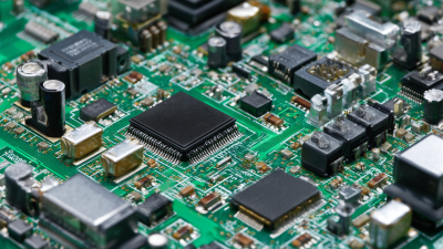
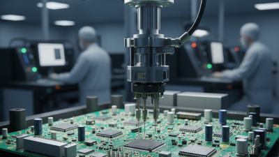
WORLD electronics offers a complete line of electronic circuit board manufacturing and assembly services, as well as advanced manufacturing services. Our commitment to quality and service is second to no supplier.
Learn MoreOur team of engineers assists you in the development of new designs to optimize quality manufacturability (DFM) and testability, resulting in cost minimization and reduced product development time.
Learn MoreOur flexible manufacturing floor layout and highly trained staff allow for Quick Set-up and Tear Down of small volume prototype runs. This combination grants our customers the benefit of turning new designs quickly and accurately.
Learn MoreWORLD electronics is dedicated to quality. This quality is what underpins our commitment to thorough testing. Our engineers can develop a set of tests that ensure reliability and high performance in all products.
Learn MoreSupply chain management has crossed over from being a narrow management function to being a key operational function.
Learn MoreA pcb assembly board is a populated circuit board designed to control, connect, and power electronic functions. It begins as a bare PCB with copper pathways, insulating layers, and drilled mounting holes. Manufacturers then place components such as resistors, capacitors, integrated circuits, connectors, and sensors onto its surface.
Tiny solder joints secure these parts and create reliable electrical connections. Some assemblies use surface-mount technology, while others include through-hole components for mechanical strength. During operation, electrical signals travel along copper traces between components. Power reaches the circuit through designated rails, while control signals follow carefully designed routes. The result may be found inside a medical instrument, industrial controller, appliance, or communication device.
A dependable assembly requires more than accurate placement. Engineers review schematics, thermal limits, component availability, and manufacturing tolerances before production. Automated optical inspection can detect missing parts, reversed components, or uneven solder. Functional testing then checks whether the completed board performs as intended. Standards such as IPC guidance can support consistent workmanship, although compliance alone does not guarantee perfect field performance.
Real-world failures still happen. A clean-looking board can contain a weak solder joint or a component affected by heat. This is where practical testing matters. Engineers compare test results with design expectations and investigate unusual behavior instead of assuming the process worked. Understanding how a pcb assembly board is built and operates helps readers judge quality, troubleshoot faults, and communicate more clearly with designers and manufacturers.
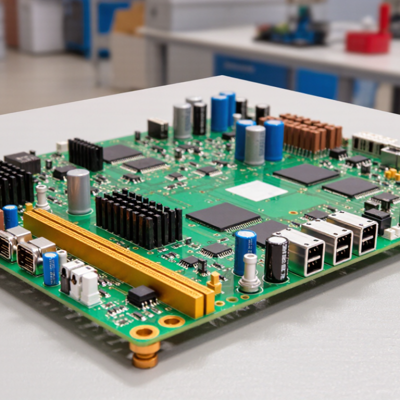
A PCB assembly board begins as a printed circuit board, or PCB. The bare board contains copper traces, pads, vias, and insulating layers. These features create controlled paths for electrical current. During assembly, solder paste is applied to the pads. Components are then placed with precise alignment. Heat melts the paste and forms solder joints. The result is a PCBA, or printed circuit board assembly.
The distinction matters. A PCB has no installed components, while a PCBA can perform a circuit’s intended function. IPC-6012 defines qualification and performance requirements for rigid printed boards. It addresses construction, materials, testing, and acceptance conditions. However, it does not replace the assembly drawing or the complete manufacturing process. Engineers still need to define board class, copper thickness, hole quality, and inspection criteria.
A practical inspection may include automated optical inspection, electrical testing, and X-ray review of hidden joints. Small details matter. A slightly lifted component can interrupt power or create intermittent faults. A board may pass a visual check yet fail during vibration or temperature changes. Standards improve consistency, but they do not remove judgment. In real production, unclear drawings and rushed reviews remain common weaknesses. IPC-6012 helps expose these risks, especially when test records, material certificates, and process controls are kept together.

A PCB assembly combines a printed circuit board with electronic components. Copper layers form the conductive paths, while the IPC-6012 standard defines performance and qualification requirements for rigid printed boards.
The values use the standard relationship between copper weight and nominal copper thickness: 1 oz/ft² is approximately 34.3 µm. In production, the finished conductor thickness can differ because of plating, etching, and manufacturing tolerances. These factors are evaluated together with other board requirements under the applicable IPC-6012 performance class.
What Is a PCB Assembly Board and How Does It Work?
A PCB assembly board combines a fabricated circuit board with soldered electronic components. Its base is often FR-4, a glass-fiber and epoxy laminate specified under IPC-4101E. The material provides mechanical strength and electrical insulation. A multilayer board may contain signal, power, and ground layers. Thin copper planes connect them through plated vias. The layer stack controls impedance, heat flow, and routing space.
One ounce copper is a practical starting point for many control and consumer boards. IPC-4562 defines this foil as approximately 305 g/m², or about 35 µm before processing. Etching reduces the final trace width, while plating can increase copper thickness inside holes and on exposed features. The number matters. A narrow 35 µm trace carries less current than a wide copper pour. Designers should use IPC-2221 calculations for current capacity and temperature rise. A common mistake is treating “1 oz” as an exact finished thickness. It is nominal, not absolute.
Tips: Confirm the laminate’s glass-transition temperature, dielectric thickness, and copper tolerance with the fabricator. Check the finished cross-section, not only the CAD stack-up. Thermal testing is also valuable. FR-4 can survive normal assembly temperatures, but repeated heating may reveal weak vias or poor design margins. That detail deserves review.
| Data Dimension | Typical Specification | Role in the PCB Assembly | Engineering Notes |
|---|---|---|---|
| Base material | FR-4 glass-reinforced epoxy laminate | Provides mechanical support and electrical insulation for copper circuitry. | FR-4 is a flame-retardant laminate system; its exact resin content and performance depend on the selected material grade. |
| Common board structure | 2-layer or 4-layer construction | Routes signals, power, and ground between component connection points. | Layer count increases routing capacity and can improve power distribution and electromagnetic compatibility. |
| Copper weight | 1 oz per ft² | Forms conductive traces, pads, planes, and plated interconnections. | Nominal rolled or deposited copper thickness is approximately 35 µm before additional plating or processing. |
| Copper resistivity | Approximately 1.68 × 10⁻⁸ Ω·m at 20 °C | Determines voltage drop, power loss, and heat generation in conductive paths. | Actual resistance also depends on trace length, width, thickness, temperature, and surface finish. |
| Dielectric layers | FR-4 prepreg and core material | Separates copper layers and controls electrical insulation and impedance. | Finished dielectric thickness varies with glass style, resin content, pressing conditions, and design requirements. |
| Typical board thickness | Approximately 1.6 mm for a standard rigid board | Provides rigidity and establishes the mechanical envelope for assembly installation. | Other thicknesses are possible; the final value includes laminate, copper, solder mask, and surface-finish contributions. |
| Solder mask | Polymer coating over most exposed copper | Reduces accidental solder bridging and protects copper from contamination and oxidation. | Pads and other designated contact areas remain uncovered for soldering or electrical connection. |
| Surface finish | Electroless nickel immersion gold, immersion tin, or lead-free hot-air solder leveling | Improves solderability and protects exposed copper pads during storage and assembly. | The selected finish affects shelf life, contact performance, cost, and compatibility with the assembly process. |
| Through-hole vias | Plated holes connecting selected or all copper layers | Create vertical electrical paths between layers and may also support component leads. | The hole wall is made conductive by copper plating; drill size and aspect ratio affect manufacturability. |
| Surface-mount pads | Copper land patterns defined by component package geometry | Provide solderable electrical and mechanical connections for surface-mount components. | Pad size, spacing, solder-mask clearance, and stencil aperture design influence solder-joint quality. |
| Assembly method | Surface-mount technology, through-hole technology, or a combination | Attaches electronic components to the fabricated bare board. | Surface-mount parts are commonly placed with automated equipment; through-hole parts may be soldered by wave or selective methods. |
| Electrical function | Signal routing, power distribution, grounding, and interconnection | Connects components so the assembled circuit can process, control, or distribute electrical energy. | The PCB itself is generally passive, although embedded components and specialized structures can add functionality. |
| Thermal behavior | Heat conducted through copper and dissipated through board and component interfaces | Helps manage heat produced by current flow and active components. | Thermal vias, copper planes, wider traces, and external heat sinks can improve heat removal. |
| Quality verification | Visual inspection, automated optical inspection, electrical test, and functional test | Checks fabrication accuracy, component placement, solder joints, and circuit operation. | The appropriate test method depends on board complexity, production volume, accessible test points, and product risk. |
A PCB assembly board is a bare circuit board populated with electronic components. It connects resistors, processors, sensors, and connectors through copper pathways. Component mounting determines how accurately and reliably those parts become a working circuit. Surface-mount technology, or SMT, places components directly onto copper pads. Through-hole technology, or THT, inserts component leads through drilled holes.
SMT supports compact designs and fast automated production. The 0201 package measures only 0.6 × 0.3 mm, smaller than a grain of rice. A stencil applies solder paste to precise pads, then a placement machine positions each component. Heat melts the paste and forms the solder joints. Very small.
At this scale, a minor stencil error can create insufficient solder or a hidden bridge. Uneven board surfaces can also shift components during reflow. Optical inspection helps detect placement problems, but it cannot replace careful process control. Technicians often check paste volume, component alignment, temperature profiles, and pad cleanliness. THT remains useful for larger parts that face mechanical stress, such as terminals or switches. Its leads provide strong physical support, although drilling and manual insertion can increase production time. Neither method is automatically better. The correct choice depends on size, heat exposure, assembly volume, and expected mechanical loads. In practice, mixed SMT and THT designs are common, yet the transition between both methods requires thoughtful spacing and inspection.
A PCB assembly board combines a bare circuit board with soldered electronic components. Copper traces carry electrical signals, while pads provide mechanical and electrical connections. During assembly, solder paste holds components in position before heat permanently joins them to the board.
SAC305 solder paste contains tin, silver, and copper. It begins melting at approximately 217°C, so a reflow profile must control heat carefully. The board first warms gradually, allowing moisture and solvents to escape. A short soak helps equalize temperatures across large copper areas and small components.
The peak temperature usually rises above the melting point, often around 235–250°C, depending on the paste and component limits. Too little heat can produce weak joints. Too much heat may damage sensitive parts or warp the board.
Inside the reflow oven, molten solder wets the component leads and copper pads. Surface tension can pull small parts into alignment, but it cannot correct every placement error. After cooling, the solder forms a solid joint and creates an electrical path through the circuit. Technicians inspect joint shape, voids, bridging, and insufficient wetting using optical or X-ray methods. In practical production, a profile that looks correct on paper may still fail because board thickness and copper weight change heat transfer. I have found that minor temperature adjustments sometimes improve results, but careless changes create new defects. Careful measurement remains essential.
A PCB assembly board combines a bare circuit board, electronic components, and soldered connections. Quality control verifies that these parts work together safely. Automated optical inspection, or AOI, uses cameras to examine solder bridges, missing components, polarity marks, and misaligned parts. It detects visible defects quickly.
In-circuit testing, known as ICT, checks electrical behavior at specific test points. It can identify open circuits, short circuits, incorrect values, and damaged components. Test fixtures must contact the board accurately. Poor contact can create a false failure. Small components matter.
X-ray inspection examines hidden solder joints beneath packages and connectors. It can reveal voids, poor wetting, cracks, and misplaced internal connections. This method is especially useful when visual inspection cannot reach the joint. Still, inspection is not infallible. A clean image may hide a process problem that appears later during temperature cycling.
IPC-A-610 provides widely used visual acceptance criteria for electronic assemblies. It covers solder shape, component placement, conductor condition, and workmanship. Different product classes require different acceptance levels. Inspectors should record defect images, measurements, and repair decisions. Relying on one method is a weakness. AOI, ICT, X-ray results, operator checks, and process records should support one another. In practice, even experienced teams must review borderline joints carefully, because lighting, component geometry, and solder appearance can mislead judgment.